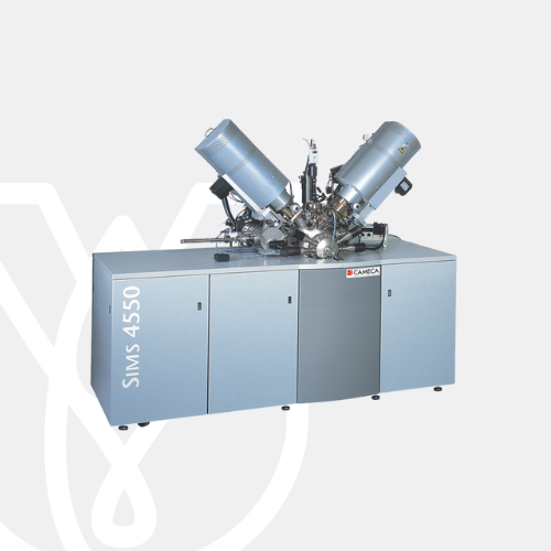
SIMS 4550
Quadrupole SIMS Dopant Depth Profiling and Thin Layer Analysis in Semiconductors
The CAMECA SIMS 4550 offers extended capabilities for ultra shallow depth profiling, trace element and composition measurements of thin layers in Si, high-k, SiGe and other compound materials such as III-V for optical devices.
High depth resolution and high throughput
With ever shrinking device dimensions, the implant profiles and layer thickness of today’s semiconductors are often in the range of 1-10nm. The SIMS 4550 has been optimized to address these application fields by offering oxygen and cesium high density primary beam with an impact energy programmable from 5keV down to less than 150eV.
Flexibility
CAMECA’s SIMS 4550 is a dynamic SIMS tool offering full flexibility in sputter conditions (impact angle, energy, species). With dedicated options for charge compensation (electron gun, laser) during sample sputtering, insulating materials can be easily analyzed. The SIMS 4550 measures layer thickness, alignment, abruptness, integrity, uniformity and stoechiometry. Sample holders can accommodate a variety of samples: small pieces of a few mm² up to 100mm diameter sample size.
High precision and automation
State-of-the-art quadrupole analyzer optics and superior peak to background performance are key factors for low detection limits for trace elements. The SIMS 4550 offers excellent sensitivity for H, C, N and O thanks to its advanced UHV design with main chamber pressure in the low E-10mbar (E-8Pa) range. Ultra stable ion sources and electronics ensure highest precision and repeatability of measurements down to < 0.2% RSD.
The human factor on precision is well taken into consideration by easy-to-use software, predefined recipes, remote operation and trouble shooting. All instrument settings of each measurement are stored in a database. Repeated measurements are therefore only a few mouse clicks away. Further automation features
For more information about this product, click here
